In the semiconductor industry, thermal management is a non-negotiable design requirement. As equipment becomes more compact and power-dense, materials must offer not just chemical resistance or dimensional stability, but also the ability to manage heat effectively. In many applications, electrostatic dissipation is equally critical, especially where sensitive electronic components are involved. (Note: Ensinger offers specialized ESD-safe PEEK grades that combine favorable thermal conductivity with electrostatic discharge protection, helping reduce the risk of component failure and contamination in cleanroom environments.)
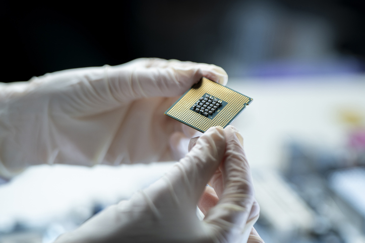
That’s where PEEK (polyether ether ketone) stands out. Known for its unique balance of mechanical, thermal, and chemical performance, PEEK is increasingly used in demanding semiconductor applications where thermal conductivity plays a critical role. From wafer handling to insulative support structures, this high-performance thermoplastic helps ensure long-term reliability, process integrity, and performance under continuous thermal load.
Why PEEK Thermal Conductivity Matters in Semiconductor Applications
Thermal conductivity is often a limiting factor in polymer component performance, especially in high-heat semiconductor environments. Unfilled PEEK typically has a thermal conductivity around 0.5 W/(m•K) — higher than many standard engineering plastics, but far lower than metals.
However, PEEK’s conductivity can be significantly enhanced through reinforcement with fillers like carbon fiber or graphite, enabling better heat dissipation without sacrificing the polymer’s mechanical integrity.
In semiconductor manufacturing, components such as wafer handling arms, test sockets, and device carriers are repeatedly exposed to high temperatures. Inadequate thermal conductivity can lead to localized overheating, which increases the risk of deformation, dimensional instability, or part failure. This is particularly critical in environments where tolerances are tight and cycles are fast.
Beyond preventing deformation, thermal stability and low thermal expansion help ensure consistent performance across thermal cycles, an essential quality in both wafer-level processing and metrology systems. Cleanroom conditions also place added demands on materials, requiring them to maintain thermal performance without outgassing or contamination. Selecting a material like PEEK — especially in its filled forms — helps mitigate these risks while meeting stringent cleanliness standards.
Advantages of PEEK Thermal Conductivity in Semiconductor Manufacturing
Thermal conductivity is only part of what makes PEEK a preferred material in semiconductor applications. Its exceptional chemical resistance ensures compatibility with acids, solvents, and etchants commonly used in wafer processing, while its ultra-low outgassing and high purity make it suitable for cleanroom use and vacuum environments.
Equally important is PEEK’s dimensional stability under thermal load. Unlike many other plastics, it resists creep and maintains its shape and function even during repeated heating and cooling cycles. Its wear resistance and mechanical strength make it a smart choice for high-friction applications like wafer grippers and component guides.
Because of its consistent performance at elevated temperatures, PEEK also supports long part life and lower replacement costs in critical equipment. Whether used as an insulative mount, structural bracket, or fluidic component, it delivers reliable function with minimal thermal or mechanical degradation, which is a key benefit in automated, high-throughput semiconductor lines.
Injection Molding High-Performance PEEK Parts
When tight tolerances and consistent part performance are required at scale, injection molding offers a repeatable and cost-effective production method for PEEK parts. This is especially true for complex designs where micro features, thin walls, or integrated geometries must be maintained across hundreds or thousands of components.
PEEK’s high processing temperature and viscosity make it more difficult to mold than standard polymers. Filled grades — especially those modified for thermal conductivity — require specialized knowledge of flow behavior, tooling design, and processing windows. Poor processing can lead to voids, inconsistent crystallinity, or warped parts that fail under heat.
That’s why it’s critical to partner with a processor experienced in high-temperature, high-performance polymers like PEEK. Ensinger specializes in molding PEEK and other engineering thermoplastics in controlled environments, supporting semiconductor OEMs with both material expertise and precision manufacturing. From prototype to production, Ensinger helps ensure that your parts deliver the thermal performance and stability your application demands.
Ensinger’s Expertise in PEEK Thermal Conductivity and Injection Molding
At Ensinger, we specialize in injection molding carbon- and glass-filled PEEK grades tailored for demanding applications like semiconductor manufacturing. Our team understands the unique flow behavior and thermal characteristics of these advanced materials, enabling us to deliver precision-molded parts with optimized thermal performance.
Our facilities include controlled molding environments and post-processing, helping ensure components meet the purity and performance requirements of semiconductor OEMs. Whether your part requires complex geometries, tight tolerances, or high heat resistance, we offer engineering support at every stage — from resin selection and part design to tooling and production.
Contact our team today to discuss your design needs or request a quote for your next high-performance project.