Semiconductor devices power the modern world, from smartphones and computers to medical equipment and automotive systems, demanding unmatched precision and reliability. At Ensinger, we deliver high-performance injection molding and machining components tailored for semiconductor manufacturing, meeting the industry’s strictest standards with precision parts like wafer handling solutions, ESD-safe housings, and custom cleanroom plastics.
Semiconductor Manufacturing Solutions
Our Materials for Semiconductor Parts and Processes
Plastics for Wet Chemical Processing
When it comes to wet chemical processing, semiconductor manufacturing solutions require plastics that withstand aggressive chemicals, maintain ionic purity, and meet strict ESD requirements. Ensinger delivers high-performance materials engineered for precision and reliability in every step of the process.
| Material | Chemical Resistance | Heat Resistance | Ionic Purity | ESD/SD Options | Suitable Processes |
| Conductive PEEK (e.g., TECAPEEK) | Excellent | Up to 260°C | High | Yes – Conductive/SD | Wet Bench, Single Wafer Etch, CMP |
| PPS (Polyphenylene Sulfide) | Excellent | Up to 220°C | High | Yes – Conductive | Electroplating, Wet Bench |
| PEI (Polyetherimide) | Good | Up to 340°C | High | Yes (SD) | Batch Spray, Coater/ Developer |
| PSU (Polysulfone) | Moderate | Up to 150°C | Moderate | Yes (SD) | Single Wafer Etch, CMP |
| POM (Polyoxymethylene, e.g., TECAFORM) | Good | Up to 180°C | Moderate | Yes (SD) | Batch Spray, Coater/ Developer |
| PET (Polyethylene Terephthalate) | Moderate | Up to 110°C | Moderate | Optional | Wet Bench, Electroplating |
| PC (Polycarbonate) | Moderate | Up to 140°C | Moderate | Yes (SD) | Coater/ Developer, Batch Spray |
| PVDF (e.g., TECATRON PVDF) | Excellent | Up to 140°C | High | Optional | Electroplating, Wet Bench |
| PTFE (Polytetrafluoroethylene) | Excellent | Up to 260°C | High | Optional | Single Wafer Etch, CMP |
Material Requirements: Our plastics provide chemical resistance, wear resistance, heat tolerance (~100°C and higher), ionic purity for contamination control, and ESD protection with conductive and static dissipative (SD) grades available.
Suitable For: Wet Bench, Single Wafer Etch, Batch Spray, Coater/Developer, Electroplating, and CMP applications.
Plastics for Dry Processing
Dry semiconductor processes power the precision and scalability of modern chip fabrication, relying on techniques that avoid wet chemicals for greater control at the nanoscale. At Ensinger, our high-performance plastics are engineered for these critical applications, offering exceptional thermal stability, wear resistance, and low outgassing to support processes like plasma etching, deposition, and ion implantation — all while reducing environmental impact.
| Material | Heat Resistance | Wear Resistance | Low Outgassing | ESD/SD Options | Suitable Processes |
| PI (Polyimide) | Up to 470°C | Excellent | Yes | Optional | ALD, Plasma Etching (RIE/DRIE) |
| PEEK/PBI (e.g., TECAPEEK blends) | Up to 260°C | Excellent | Yes | Yes (SD) | Deposition (PVD, ICP-PECVD), Ion Implantation |
| PAI (Polyamide-Imide) | Up to 260°C | Excellent | Yes | Yes (SD) | Ashing, RIE/DRIE |
| PEKEKK | Up to 260°C | Excellent | Yes | Optional | ICP-PECVD, ALD |
| PEEK (e.g., TECAPEEK) | Up to 260°C | High | Yes | Yes (Conductive/SD) | Plasma Etching, Deposition (PE-CVD) |
| PPS (Polyphenylene Sulfide) | Up to 260°C | High | Yes | Yes (Conductive) | PVD, Ashing |
| PEI (Polyetherimide) | Up to 340°C | Good | Yes | Yes (SD) | PE-CVD, Ion Implantation |
| PSU (Polysulfone) | Up to 150°C | Moderate | Yes | Yes (SD) | Ashing, Light Deposition |
| POM (e.g., TECAFORM) | Up to 120°C | High | Moderate | Yes (SD) | Batch Etching, Deposition |
| PET (Polyethylene Terephthalate) | Up to 140°C | Moderate | Moderate | Optional | Ashing, PVD |
| PC (Polycarbonate) | Up to 140°C | Moderate | Moderate | Yes (SD) | Ashing, Light PE-CVD |
Material Requirements: Our plastics deliver heat resistance (up to 400°C+ for extreme conditions), wear resistance for durability, low outgassing to prevent contamination in vacuum environments, and optional ESD/static dissipative (SD) properties where static control is critical.
Suitable For: Ashing, Plasma Etching (RIE/DRIE), Deposition (PVD, PE-CVD, ICP-PECVD), Atomic Layer Deposition (ALD), and Ion Implantation.
Plastics for Testing Fixtures
Testing fixtures — like test sockets and inspection jigs — are critical for ensuring the quality and reliability of semiconductor devices. At Ensinger, we provide materials designed for these precision applications, offering dimensional stability, stiffness, and durability through repeated cycles. Our plastics withstand extreme temperature swings (-60°C to nearly 200°C), maintain low outgassing, and deliver ESD protection to meet the rigorous demands of semiconductor testing.
| Material | Heat Resistance | Dimensional Stability | Wear Resistance | ESD/SD Options | Suitable Applications |
| PI (Polyimide) | Up to 250°C | Excellent | Excellent | Yes (Anti-static) | Test Sockets, Inspection Fixtures |
| PAI (Polyamide-Imide) | Up to 250°C | High | Excellent | Yes (Anti-static) | High-Cycle Test Sockets |
| PEEK (e.g., TECAPEEK) | Up to 260°C | High | High | Yes (Anti-static/SD) | Precision Inspection Jigs |
| PEI (Polyetherimide) | Up to 170°C | Good | Good | Yes (Anti-static/SD) | Test Fixtures, Contact Sockets |
Material Requirements: Our plastics offer dimensional stability with low water absorption, stiffness for machinability, wear resistance for repeated use, rigidity, low dielectric constant, low outgassing to prevent contamination, and anti-static/ESD properties. Designed to endure temperature extremes (-60°C to nearly 200°C), they ensure consistent performance in demanding test environments.
Suitable For: Test sockets, inspection fixtures, and contact jigs used in semiconductor quality assurance and control.
Conductive and ESD Plastics
Static control is critical in semiconductor manufacturing, where even minor electrostatic discharge (ESD) can damage sensitive components. At Ensinger, our conductive and ESD plastics are engineered to provide reliable static dissipation and conductivity, ensuring safety and precision across fabrication, testing, and handling processes. These materials combine high performance with tailored electrical properties to meet the industry’s toughest standards.
| Material | Heat Resistance | Material (Density) | Surface Resistivity | Tensile E-modulus |
| TECAPEEK ELS CF30 | Up to 260°C | PEEK (1.38) | 102-104 Ω/Sq | 6800 MPa |
| TECAPEEK ELS | Up to 260°C | PEEK (1.36) | 102-104 Ω/Sq | 4800 MPa |
| TECAFLON PVDF ELS | Up to 150°C | PVDF (1.78) | 102-106 Ω/Sq | 3100 MPa |
| TECAFORM AH ELS | Up to 100°C | POM (1.41) | 102-104 Ω/Sq | 1800 MPa |
| TECAPEEK SD | Up to 260°C | PEEK (1.71) | 106-109 Ω/Sq | 5800 MPa |
| TECAFORM AH SD | Up to 100°C | POM (1.35) | 109-1011 Ω/Sq | 1300 MPa |
Material Requirements: Our conductive and ESD plastics offer tailored electrical properties (conductivity or static dissipation), heat resistance (up to 260°C), wear resistance for durability, and chemical resistance where needed, ensuring compatibility with semiconductor environments while protecting against static damage.
Suitable For: Wafer handling, cleanroom components, test fixtures, inspection jigs, electrical contacts, and static-safe parts across wet and dry processing, testing, and assembly stages.
Plastics for CMP Retaining Rings
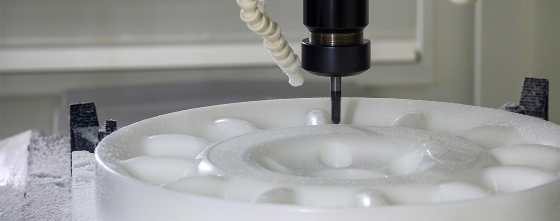
CMP retaining rings are essential for securing wafers during polishing, ensuring uniform material removal and minimizing defects. At Ensinger, our plastics for CMP retaining rings are optimized for durability, wear resistance, and dimensional stability, delivering longer service life and reduced wafer-level defects in semiconductor manufacturing.
| Material | Long-Term Temp | Tensile E-modulus | Elongation at Break | Flexural Strength | Ball Indentation Hardness |
| TECAPEEK SX natural | Up to 260°C | 4200 MPa | 15% | 175 MPa | 253 MPa |
| TECAPEEK CMP natural | Up to 260°C | 4100 MPa | 50% | 160 MPa | 240 MPa |
| TECATRON CMP natural | Up to 230°C | 4100 MPa | 4% | 151 MPa | 248 MPa |
| TECATRON SX natural | Up to 230°C | 4000 MPa | 11% | 151 MPa | 230 MPa |
| TECANAT CMP natural | Up to 120°C | 2200 MPa | 90% | 97 MPa | 128 MPa |
| TECADUR PET CMP natural | Up to 110°C | 3300 MPa | 14% | 134 MPa | 194 MPa |
Material Requirements: Our plastics provide exceptional wear resistance for extended ring life, dimensional stability to maintain tight tolerances, heat resistance (up to 260°C for high-performance grades), and chemical resistance to withstand slurry exposure, all while minimizing inner groove wear and micro-scratches on wafers.
Suitable For: CMP retaining rings used in wafer polishing across semiconductor fabrication, supporting processes requiring high precision, reduced defect rates, and optimized pad asperity performance.
Ensinger: Your Semiconductor Manufacturing Solutions Partner
At Ensinger Precision Components, we’re proud to craft high-performance plastics that power semiconductor innovation — from CMP retaining rings to ESD-safe testing fixtures. With decades of injection molding and machining expertise, we deliver tight tolerances, durability, and material excellence tailored to your wet processing, dry processing, and quality control needs.
Ready to enhance your semiconductor process? Contact our team for custom solutions that meet your exact specifications.